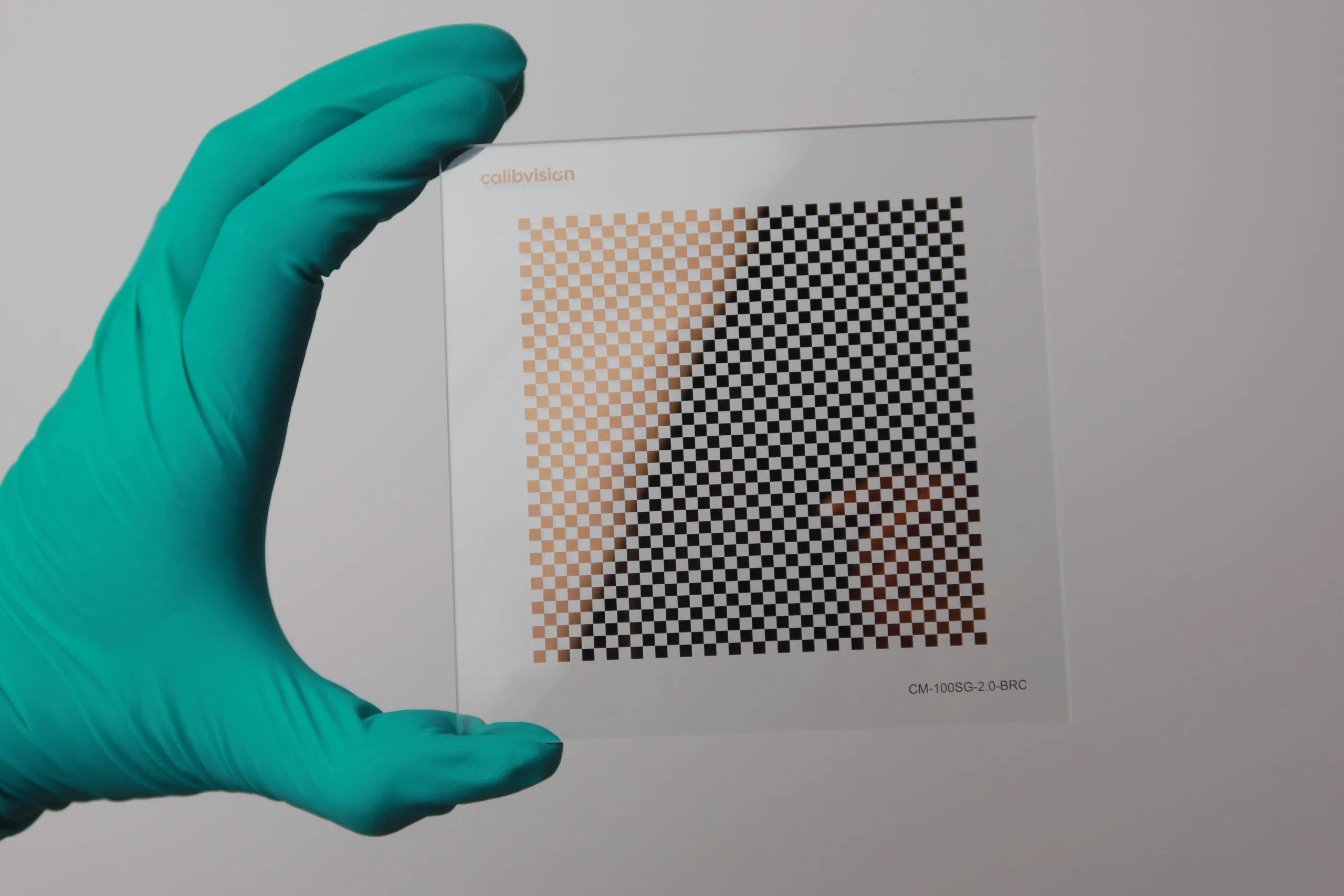
In semiconductor wafer inspection, your measurement is only as accurate as your calibration target. When you’re detecting particles smaller than 50 µm, verifying die placement to micron tolerances, or measuring kerf width after dicing, a standard ±1 µm printed checkerboard isn’t a calibration tool — it’s a source of error.
This guide covers why semiconductor metrology demands sub-micron calibration targets, what specifications actually matter, and how to specify a custom checkerboard or fiducial target that won’t become the limiting factor in your inspection system. If you already know what you need, you can request a custom quote and our engineers will respond within 24 hours.
Why Standard Calibration Targets Fail in Semiconductor Inspection
Semiconductor inspection cameras have evolved to match shrinking device geometries. Ultra-high-resolution sensors now capture features at sub-micron scale, with the pixel sizes shrinking to match the components they inspect. At this scale, three properties of a standard calibration target become deal-breakers:
- Feature accuracy. A printed or even a standard soda-lime glass checkerboard typically holds ±1 µm corner accuracy at best. The rule of thumb in metrology is that your reference should be 3–5× more accurate than the tolerance you’re measuring. If you’re verifying die placement to ±1 µm, your target needs ±0.2–0.3 µm accuracy — beyond what standard targets deliver.
- Thermal stability. Semiconductor fabs run tight temperature control, but inspection tools still see thermal cycling. Soda-lime glass expands ~8.5 µm per meter per °C. Over a 100 mm target and a few degrees of drift, that’s enough to shift your calibration. Quartz glass (fused silica) expands ~15× less — essential when your measurement budget is sub-micron.
- Edge quality for sub-pixel detection. Wafer inspection algorithms rely on sub-pixel corner or edge detection. A printed target with ink bleeding or a low-contrast edge caps your sub-pixel accuracy no matter how good your camera is. Chrome-on-glass patterns made by photolithography give the clean, high-contrast edges these algorithms need.
What Semiconductor Inspection Actually Requires
Different inspection tasks in the wafer line have different calibration needs. Here’s how target specifications map to real applications:
| Inspection Task | Typical Feature Scale | Recommended Target Spec |
| Particle / defect detection | < 50 µm particles | Quartz glass, ±0.3 µm, fine checkers (0.1–0.5 mm) |
| Die placement & alignment verification | Micron-level | Quartz glass, ±0.3 µm, custom fiducials |
| Post-dicing kerf / groove measurement | Sub-micron repeatability | Quartz glass, ±0.3 µm, fine pitch |
| Overlay metrology | Below diffraction limit | Custom sub-micron features to 0.1 µm |
| Wafer-scale stage calibration | Across 200–300 mm | Large quartz target, low CTE, custom grid |
| Probe card alignment | X-Y-Z fiducials | Custom fiducial pattern, contrast layer |
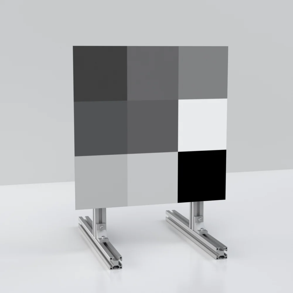
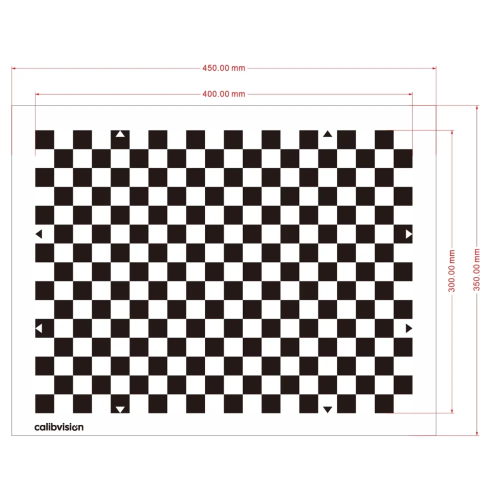
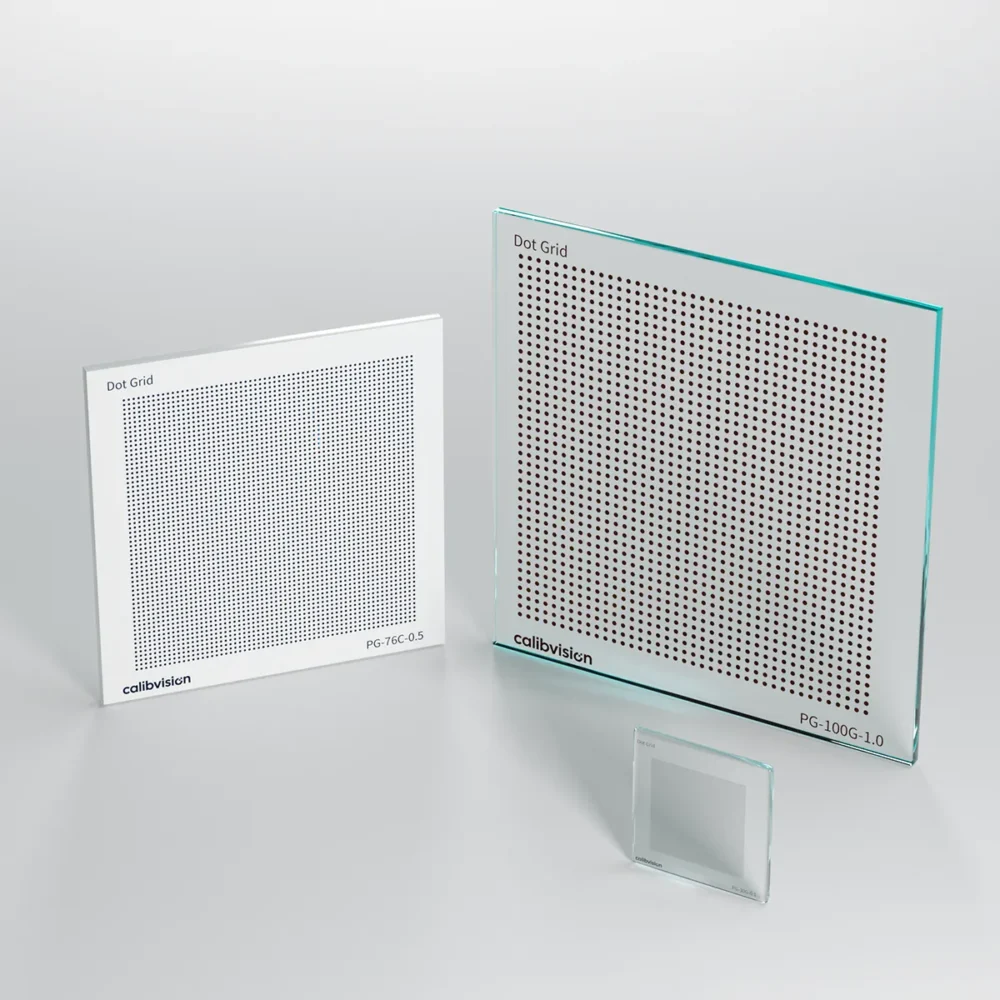
The pattern type also matters. A standard checkerboard is ideal for camera intrinsic calibration and distortion correction. But semiconductor work often needs custom fiducials, cross-hair reticles, dot grids for stage mapping, or mixed patterns that combine a calibration grid with alignment marks. This is where off-the-shelf catalog products run out, and a custom target becomes necessary.
The Specifications That Matter (and How to Specify Them)
When you request a custom semiconductor calibration target, these are the parameters to nail down:
Substrate
For sub-micron work, quartz glass (fused silica) is the default — low thermal expansion (~0.55 µm/m/°C), excellent flatness, deep-UV transmission for UV inspection systems, and chemical durability for fab cleaning protocols. Soda-lime glass works for less demanding ±1 µm tasks at lower cost. Matte ceramic suits reflective, front-lit setups where back-reflections must be eliminated.
Feature Accuracy
Calibvision manufactures to ±0.3 µm corner-position accuracy on quartz glass as standard. For overlay metrology and the most demanding applications, custom features down to 0.1 µm line width are available via direct-write laser lithography.
Pattern Design
Specify your pattern: checkerboard (and array size), dot grid, fiducials, reticle, or a custom layout. Provide a drawing in PDF, DWG, or DXF. No drawing? Our engineers offer a free design service based on your application requirements.
Flatness & Thickness
For wafer-scale targets, flatness matters as much as feature accuracy — a bowed target introduces measurement error. Quartz targets hold <1 µm flatness under 50 mm, <5 µm over 200 mm. Specify your overall size and the flatness your stage requires.
Traceability
Every target ships with a serial-numbered inspection report. For fab quality systems, NIM-traceable third-party metrology-institute calibration is available on request, providing documented traceability for your ISO/audit requirements.
Chrome-on-Glass vs Printed: Why It Matters at This Scale
For general machine vision, a printed target might be “good enough.” For semiconductor inspection, it rarely is. Calibvision uses a photolithography process — the same family of process used to make the wafers themselves:
- Substrate — high-purity quartz glass, selected for flatness
- Chrome coating — uniform, particle-free deposition
- Laser writing — direct-write lithography defines the pattern
- Developing & etching — clean, high-contrast edges with no ink bleed
- Stripping & cleaning — flawless surface
- Inspection & repair — micron-level QC on every unit
- Pellicle mounting (optional) — dust protection for fab environments
- Final QA — serial-numbered inspection report
The result is a target with crisp corners, optical-grade contrast, and the dimensional stability that sub-micron inspection demands — verified, not assumed.
How to Order a Custom Semiconductor Calibration Target
The process is built to minimize back-and-forth:
- Tell us your application — inspection task, camera/optics, required accuracy, and environment. Send a drawing (PDF/DWG/DXF) if you have one.
- Free design support — no drawing? Our engineers design the pattern to your specification and you confirm before production.
- Quote within 24 hours — detailed quotation covering substrate, pattern, accuracy, and traceability options.
- Manufacturing & QC — photolithography production with inspection report; NIM-traceable calibration if required.
- Worldwide shipping — delivered with full documentation.
Request a custom quote → Our sales engineers respond within 24 hours, typically faster.
Frequently Asked Questions
What accuracy do I need for semiconductor wafer inspection?
As a rule, your calibration target should be 3–5× more accurate than the tolerance you measure. For micron-level die placement or kerf measurement, choose ±0.3 µm (quartz glass). For overlay metrology below the diffraction limit, custom features down to 0.1 µm are available.
Why quartz glass instead of soda-lime glass for semiconductor work?
Quartz glass (fused silica) has ~15× lower thermal expansion, better flatness, and deep-UV transmission. In sub-micron inspection where thermal drift and flatness directly affect your measurement budget, quartz is the reliable choice. Soda-lime glass is suitable for less demanding ±1 µm tasks.
Can you make custom fiducials and mixed patterns, not just checkerboards?
Yes. We manufacture custom checkerboards, dot grids, cross-hair reticles, fiducials, and mixed layouts combining calibration grids with alignment marks. Send a drawing or let our engineers design it.
Do you provide traceable calibration certificates?
Every target ships with a serial-numbered inspection report. NIM-traceable third-party metrology-institute calibration is available on request for fab quality and audit requirements.
What’s the smallest feature you can make?
Custom features down to 0.1 µm line width via direct-write laser lithography on quartz glass.
How long does a custom semiconductor target take?
You receive a quotation within 24 hours of submitting your requirements. Production time depends on substrate, pattern complexity, and traceability options — typically a few weeks for custom sub-micron work.
Related Resources
- Checkerboard Calibration Targets — ChessMark Series — standard catalog, ±0.3 µm quartz
- How to Choose a Checkerboard Size for Camera Calibration — sizing guide
- Custom Calibration Targets — Order Process
- Request a Custom Quote